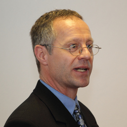
Alexander Ippich
Angestellt, Technical Director, Signal Integrity & Advanced Technology, Isola Group
Dueren, Deutschland
Werdegang
Berufserfahrung von Alexander Ippich
Bis heute 6 Jahre und 11 Monate, seit Juni 2017
Technical Director, Signal Integrity & Advanced Technology
Isola Group
• technical point of contact for customers for all questions on Isola's material offerings and signal integrity and RF questions • generation of very high frequency electrical characterization data on Isola's materials • represent Isola on conferences and workshops • responsibility for web site content for RF products • MarCom for RF products • in charge of diploma thesis student, working on Dk/Df testing
2 Jahre und 6 Monate, Jan. 2015 - Juni 2017
Senior Signal Integrity Engineer - OEM Marketing
Isola Group
• technical point of contact for customers for all questions on Isola's material offerings and signal integrity and RF questions • generation of very high frequency electrical characterization data on Isola's materials • represent Isola on conferences and workshops • installation of IPC-TM650 2.5.5.5, Bereskin Stripline and Split-Post-Dielectric Resonator testing in Dueren facility • customer visits
1 Jahr und 4 Monate, Sep. 2013 - Dez. 2014
Sr. Development Engineer - Electronic Circuits and PCBs
Feinmetall
• technical point of contact for customers for all electrical questions • responsibility for specification of printed circuit boards for wafer probe cards • characterization of the electrical properties of various connector technologies for wafer probe cards • technical support of quality department regarding claims (electrical issues and PCB issues) • customer visits / on-site debugging
3 Jahre und 11 Monate, Okt. 2009 - Aug. 2013
Sr. Signal Integrity Engineer
Multek
•corporate resource for all Multek facilities (Brazil, US, Germany, China) •technical point of contact for all electrical questions of our customers •electrical base material characterization •insertion loss testing with VNA, SPP, SET2DIL •presentations on electrical topics to customers •paper publication and presentation for international conferences
3 Monate, Aug. 2012 - Okt. 2012
Acting Application Engineering Manager
Multek
•technical lead for the team of 6 application engineers •technical customer support and meetings •liaison to upper management
7 Jahre und 2 Monate, Sep. 2002 - Okt. 2009
Senior Application Engineer / Customer Team
Multek
•responsible for all technical questions of various customers •computing: 3 large server manufacturers •medical: 2 implantable medical device makers, one disposable medical device maker •technical point of contact for Multek Germany customers for all electrical questions
7 Monate, März 2002 - Sep. 2002
Acting Application Engineering Manager
Multek
•technical lead for the team of 8 application engineers •reporting of performance measures of the group •liaison to upper management
3 Jahre und 7 Monate, Sep. 1998 - März 2002
Senior Application Engineer / Electrical Team
Multek
•technical point of contact for Multek Germany customers for all electrical questions •stackup generation •promoted to Senior Application Engineer 11/2000
1 Jahr und 3 Monate, Juli 1997 - Sep. 1998
New Process and Product Engineer
Hewlett-Packard
•responsible for implementation of new electrical screening procedures of blank boards •calculation of PCB stackups according to customer requirements •optimization of stackups for impedance controlled multilayers •'baby-sitting' of prototypes with new processes •customer support - electrical issues with blank boards •training of operators
2 Jahre und 7 Monate, Jan. 1995 - Juli 1997
R&D Engineer
Hewlett-Packard
•programming of HP54121 and HP54750/54753 TDR tools; implementation of 100% measurement for volume production •measurements of impedance, propagation delay and crosstalk with HP8510 network analyzer and HP54121 time domain reflectometer •electrical characterization of standard and new PCB base materials •implementation of impedance simulations •crosstalk simulations with HFSS and SSpice •tooling & production of micro via PCBs •customer support - electrical issues with blank boards
10 Monate, Juni 1994 - März 1995
Diploma Thesis: Production of a-Si-TFT with Channel Etch-Stop
Universitaet Stuttgart - Institute for Network and System Theories
• usage of photo lithography, sputtering, PECVD, ion implanting, plasma etching and RIE etching to produce a-Si-TFT on glass substrates for usage in LCD displays • extensive work under clean room conditions • measurement of the electrical characteristics of the TFTs
6 Monate, Nov. 1993 - Apr. 1994
Graduate Work: Impedance Measurement and Design of Testboards
Hewlett-Packard
• impedance measurements on PCBs • impedance calculations • design and production of test boards • tooling of micro via test samples
8 Monate, Apr. 1993 - Nov. 1993
Graduate Work: Production of LCD Cells and Measurement of the Optical Char.
Universitaet Stuttgart: Institute for Network and System Theories
• usage of photo lithography, sputtering, PECVD, plasma etching and RIE etching to produce liquid crystal test cells • extensive work under clean room conditions • measurement of the optical characteristics of the liquid crystal test cells
6 Monate, Okt. 1992 - März 1993
Graduate Work: Training of Neuronal Nets to Predict Electrical Fields
Universitaet Stuttgart: Institute for High Frequency Technology
• training of neuronal nets to allow a prediction of electrical fields in a city environment; usage to optimize distribution of transmitters for cell phones • comparison of results with standard formulas
Ausbildung von Alexander Ippich
1989 - 1995
Electrical Engineering
Universitaet Stuttgart
specializing in RF, transmission theory
Sprachen
Englisch
Fließend
Deutsch
Muttersprache
