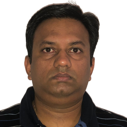
Arvind Anche
Angestellt, Deputy Head or Team Lead, Vermes Microdispensing GMBH, Munich
Abschluss: Bachelor of Engineering in Instrumentation and Electronics, Bangalore University
Munich, Deutschland
Werdegang
Berufserfahrung von Arvind Anche
Bis heute 5 Jahre und 9 Monate, seit Sep. 2018
Deputy Head or Team Lead
Vermes Microdispensing GMBH, Munich
Print Head Controller FPGA Prototyping hardware components selection for FPGA prototyping Digital design and RTL implementation and software development to evaluate on the FPGA board. Setup the verification environment for the Avalon MM Master BFM. Verification test plan development and test case implementation using System Verilog. C based application development and proof of concept on the FPGA platform. Linux Kernel, U-Boot, Angstrom Root FIle System
V93000 Advantest Tester software release management. Compatibility testing before releasing the SmarTest7 or SmarTest8. Work with RedHat5 and RedHat7. Quality checks of software release management using the online testers, customer design board and test vectors. Develop, enhance and debug existing Test applications based on new feature developments in SmarTest in both Java and C++. General V93000 Tester maintenance, Calibration and diagnostics. Effective reporting of results, test coverage, bugs found.
RTL Coding with System Verilog. Perform RTL quality checks: CDC, Lint & DFT. Developed SDC & UPF synthesis constraints for the IP/SOC. Created clock gating constraints and DFT constraints. Verification using VMM methodology. Complete ownership of IP generation, integration and system level verification of external Bus Interface (EBI) module. Developed test plans and test cases at the system level. Generation of functional and DFT test vectors to run on silicon on Advantest Tester. Support FPGA prototype.
System level integration of various IP’s in an ARM based SoC. IO pin sharing in various functional and DFT modes. Verification planning for system level verification of various IPs, test case development. Delivery of good quality RTL to synthesis team with appropriate SDC constraints. GLS setup and execution of selected functional and DFT test vectors.
Design and implementation of Digital Baseband Receiver. Interfacing with Sigma Delta ADC. Extract the binary bit pattern using manchester encoding or NRZ encoding. Implement pattern matching to start the reception of packet. Implemented the Gardner Timing Error Detection (GTED) and Matched filter to synchronise and apply corrections to incoming data reception. RTL Coding, Functional verification and FPGA prototyping performed. RTL design and gate level Verification of the I2S, I2C peripherals
Emmy , Infineon, Singapore Delivery of complete SoC RTL design for synthesis and verification. System level integration of various peripheral IP’s in an ARM based SoC. IO pin sharing in various functional and DFT modes. Verification planning and system level test cases development. Team progress reporting to customer with quality metrics for verification and RTL integration.
10 Monate, Okt. 2002 - Juli 2003
Engineer
Bisecure Networks Pvt Ltd
AES encryption and decryption algorithm Design and implementation of AES encryption and decryption algorithm IP in Verilog. Verification Planning and test case development for complete AES IP. Implementation and prototyping of the complete system on Xilinx FPGA platform.
1 Jahr und 9 Monate, Okt. 2000 - Juni 2002
Engineer
Bisquare Technologies Pvt Ltd
OCP to AHB bridge IP Delivery of OCP to AHB bridge IP RTL for the Sonics Bus infrastructure as design engineer. Verification Planning and test case development for the IP.
Ausbildung von Arvind Anche
5 Jahre, Apr. 1995 - März 2000
Instrumentation and Electronics
Bangalore University
Mathematics, Digital Electronics, Control Systems, Engineering Physics, Engineering Chemistry, Measurement Techniques, Analog Devices and circuits, Electronic Instrumentation, DSP, Signals and Systems (sampling theorem), Computer Organisation and architecture, Introduction to Microprocessors
2 Jahre, Apr. 1993 - März 1995
Computer Science
Bangalore University
Languages: English and Sanskrit Science subjets: Physics, Chemistry, Mathematics and Biology
1 Jahr, Apr. 1992 - März 1993
Computer Science
Bangalore University
Languages: Sanskrit, English and Kannada Core Subjects: Mathematics, Science and Social Studies
Sprachen
Deutsch
Grundlagen
Englisch
Muttersprache
Hindi
-
Kannada
-
Sanskrit
-
