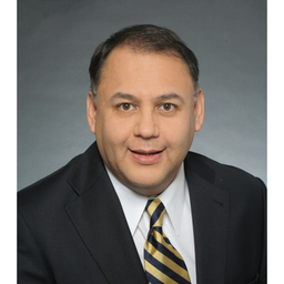

Dr. Francisco Sanchez
Suchst Du einen anderen Francisco Sanchez?
Fähigkeiten und Kenntnisse
Werdegang
Berufserfahrung von Francisco Sanchez
- Bis heute 6 Jahre und 8 Monate, seit März 2020
Regional Sales Manager
Kurt J. Lesker Company
Management and coordination of sales activities in Germany's Northern and Western regions.
Work on improving German skills.
- 5 Jahre und 9 Monate, Jan. 2014 - Sep. 2019
Applications Specialist
Nova Measuring Instruments
Support to customers in advanced application solutions in metrology inspection for the semiconductor manufacturing processes by using modeling and multi-parameter optimization techniques. Customers are based in Germany, and France.
R&D Manager for PECVD technologies. Development of new films for Anti-Reflecting and Passivation applications for crystalline Solar Cells. Active participation in trade-fairs, and conducted market research to investigate new business opportunities.
- 4 Jahre und 11 Monate, Juli 2005 - Mai 2010
Field Process Engineer
Novellus Systems
Pre- and Post Sales Support . Project coordination for the development of dielectric thin film technologies for IC customers for advanced IC devices. Work with Plasma Assisted CVD techniques.
- 1 Jahr und 4 Monate, März 2004 - Juni 2005
Research Assistant
Institut des Nanotechnologies de Lyon (INL), Lyon, France.
Member within “NanoCMOS” European research program. Responsible of conducting the epitaxial activities of oxides by Molecular Beam Epitaxy (MBE) and e-beam evaporation techniques. Worked in epitaxial high k oxide thin films on Si for advanced CMOS devices.
- 2 Jahre und 2 Monate, Jan. 2002 - Feb. 2004
Research Assistant
INFM, Dip. di Fisica G.Galilei. Padova, Italy
Member within “SiGeNet” European research program. Leaded and executed the characterization of SiGe alloys and nanostructures by Secondary Ion Mass Spectroscopy (SIMS) and Rutherford Backscattering (RBS)
- 1 Jahr, Jan. 2001 - Dez. 2001
Research Assistant
WSI - Technische Universität München, Germany
Growth of III-V alloys by Chemical Beam Epitaxy for semiconductor laser applications.
- 4 Jahre und 3 Monate, Okt. 1996 - Dez. 2000
PhD preparation
Institut des Nanotechnologies de Lyon (INL), Ecole Centrale de Lyon, France.
PhD thesis preparation on epitaxial III-V semiconductor thin films by Molecular Beam Epitaxy (MBE).
- 1 Jahr und 9 Monate, Jan. 1995 - Sep. 1996
R & D engineer
Motorola Semiconductors
Worked with Silicon technology which included oxidation, dopant-diffusion, photolithography, and metallization processes. Leaded the Thyristor wafer Fab conversion technologies from 3” to 4” wafer size.
Ausbildung von Francisco Sanchez
- 4 Jahre und 3 Monate, Okt. 1996 - Dez. 2000
Materials Science
Ecole Centrale de Lyon
Molecular Beam Epitaxy of III-V semiconductors for optoelectronic applications (LEDs, photodectectors, solar cells).
Sprachen
Französisch
C1 (Fließend)
Englisch
C1 (Fließend)
Italienisch
B1-B2 (Gute Kenntnisse)
Deutsch
B1-B2 (Gute Kenntnisse)
Spanisch
C2 (Verhandlungssicher / Muttersprachlich)
XING Mitglieder mit ähnlichen Profilangaben
XING – Die Jobbörse
Über eine Million Jobs
Entdecke mit XING genau den Job, der wirklich zu Dir passt.
Persönliche Job-Angebote
Lass Dich finden von Arbeitgebern und über 20.000 Recruiter·innen.
21 Mio. Mitglieder
Knüpf neue Kontakte und erhalte Impulse für ein besseres Job-Leben.
Kostenlos profitieren
Schon als Basis-Mitglied kannst Du Deine Job-Suche deutlich optimieren.