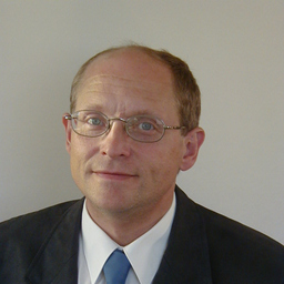

Günter Hoffmann
Suchst Du einen anderen Günter Hoffmann?
Fähigkeiten und Kenntnisse
Werdegang
Berufserfahrung von Günter Hoffmann
Electronics Development Light Microscopy Materials
R&D support for wafer inspection systems. Development of electrical and electronical subsystems for mask handling systems until series and international customer service support.
- 3 Jahre und 1 Monat, Feb. 2006 - Feb. 2009
Electronics designer
Vistec Semiconductor Systems Jena GmbH
Development and customer service support for wafer inspection systems. Computer and control systems for wafer backside inspection.
- 7 Jahre und 11 Monate, Apr. 1998 - Feb. 2006
Electronics designer
Leica Microsystems Jena gmbH
Development of electrics and electronics for thin film measurement systems and wafer inspection systems until series production.
- 9 Monate, Juli 1997 - März 1998
Electronics designer
Jenoptik Silmetric GmbH
System engineering and customer service support for wafer inspection systems.
- 1 Jahr und 3 Monate, Apr. 1996 - Juni 1997
Electronics designer
Jenoptik Infab GmbH
Electronics and system engineering for semiconductor inspection and wafer handling systems.
- 8 Monate, Aug. 1995 - März 1996
Electronics designer
Jenoptik Microfab GmbH
Electronics and PCB design for wafer handling and wafer inspection systems and international customer service support.
- 3 Jahre und 9 Monate, Nov. 1991 - Juli 1995
Electronics designer
Jenoptik Technologie GmbH
Electrics and electronics development for thermal wave inspection and wafer inspection systems.
- 10 Monate, Jan. 1991 - Okt. 1991
Electronics designer
Jenoptik Carl Zeiss Jena GmbH
PCB development and electrical design of autofocus system for waferstepper
- 5 Jahre und 4 Monate, Sep. 1985 - Dez. 1990
Scientific technical assistent for electronics
VEB Carl Zeiss Jena
PCB and test stand development for military and semiconductor systems
- 2 Jahre, Sep. 1980 - Aug. 1982
Electrician for maintenance services
Deutsche Reichsbahn
Electrician for locomotives
Ausbildung von Günter Hoffmann
- 3 Jahre und 1 Monat, Sep. 1982 - Sep. 1985
Elektronik-Entwicklung
Ingenieurschule für Elektronik und Informationsverarbeitung Görlitz
Sprachen
Englisch
B1-B2 (Gute Kenntnisse)
Deutsch
C2 (Verhandlungssicher / Muttersprachlich)
Russisch
A1-A2 (Grundkenntnisse)
XING Mitglieder mit ähnlichen Profilangaben
XING – Das Jobs-Netzwerk
Über eine Million Jobs
Entdecke mit XING genau den Job, der wirklich zu Dir passt.
Persönliche Job-Angebote
Lass Dich finden von Arbeitgebern und über 20.000 Recruiter·innen.
21 Mio. Mitglieder
Knüpf neue Kontakte und erhalte Impulse für ein besseres Job-Leben.
Kostenlos profitieren
Schon als Basis-Mitglied kannst Du Deine Job-Suche deutlich optimieren.